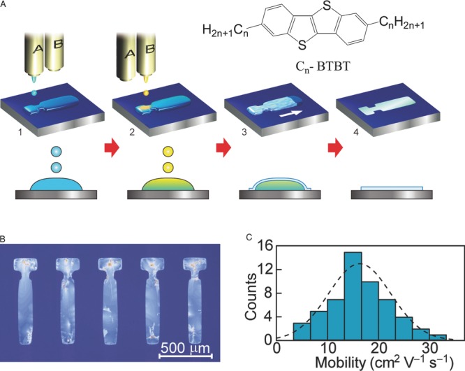
Figure 4.

Double-shot inkjet printing process of Cn-BTBT films: A) schematic diagram of process printing subsequently ink droplets of an antisolvent (blue) and then droplets of the ink comprising the organic semiconductor (yellow) onto a substrate with a surface energy pattern confining the ink droplets; the inset shows the molecular structure of Cn-BTBT; B) polarized optical micrograph of printed C8-BTBT films; C) histogram of field-effect mobilities across 54 top-gate, top-contact transistors. Reproduced with permission.[44] Copyright 2008, Macmillan Publishers Ltd.
