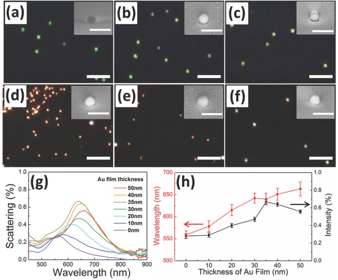
Figure 2.
Dark field images of Au NPs on (a) Si wafer, and inside Au films with different thicknesses: (b) 10 nm, (c) 20 nm, (d) 35 nm, (e) 40 nm, and (f) 50 nm (scale bars 5 μm). Insets show the corresponding SEM images (scale bars 200 nm). (g) Scattering spectra of Au NPs with evaporated Au films of different thicknesses. (h) Change of peak position and scattering intensity as a function of Au film thickness.

