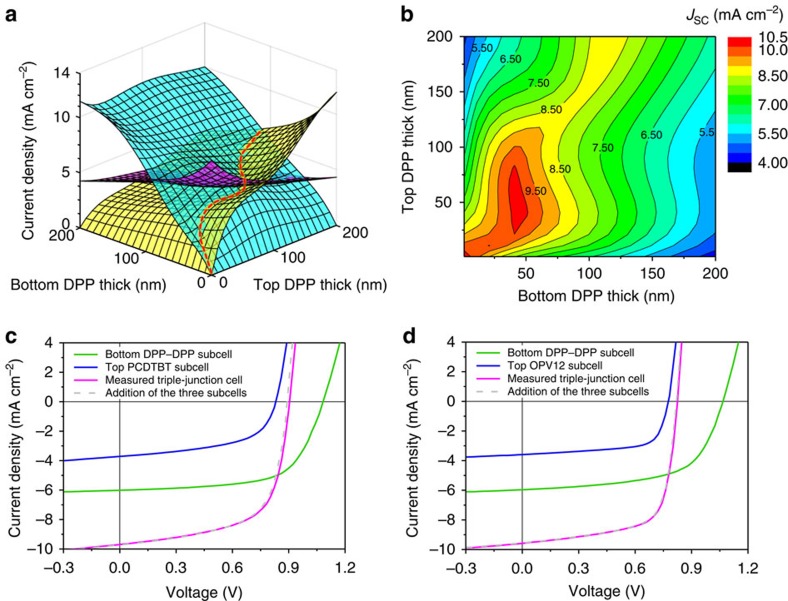
Figure 5. Optical simulations and photovoltaic characteristics of the SP triple-junction solar cells.
(a) Simulated current density distribution of the three subcells as a function of the thicknesses of bottom two DPP:PC60BM layers. (b) Contour plot of current density distribution of the entire triple-junction devices (DPP–DPP/PCDTBT) as a function of the thicknesses of bottom DPP:PC60BM layers. Note that in these two simulations the top PCDTBT:PC70BM layer thickness is fixed to 80 nm, corresponding to the optimized thickness in their single-junction state. (c,d) J–V characteristics of the investigated triple-junction cells and the constituent bottom series-tandem subcells and top subcell, (c) DPP–DPP/PCDTBT, (d) DPP–DPP/OPV12. The light grey dashed lines indicate the numerical addition of the bottom series-tandem subcells and the top subcell.

