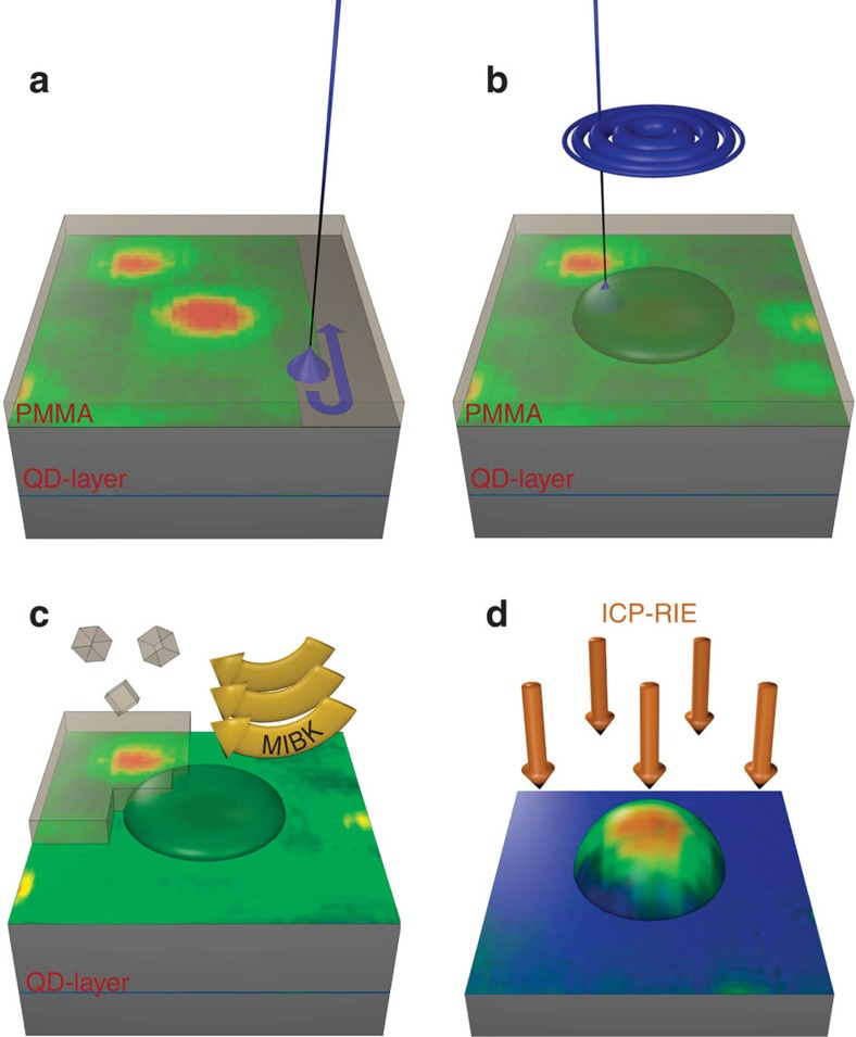
Figure 1. The lens fabrication process.
(a) The sample's luminescence is mapped by cathodoluminescence spectroscopy. Along this, the resist is exposed to an electron dose around 10 mC cm−2 and becomes soluble upon development. (b) On top of suitable QDs, lens structures are written into the resist by cross-linking the afore cracked PMMA chains by using an additional electron dose. The lens shape is defined by writing concentric circles into the resist and by carefully adjusting the respective electron doses. (c) Singly exposed resist is removed by applying the solvent methylisobutylketon and the lens shape forms in the inverted regions. (d) Upon dry etching the lens profile is transferred from the inverted PMMA into the semiconductor. The bottom DBR section is omitted for a better display format.

