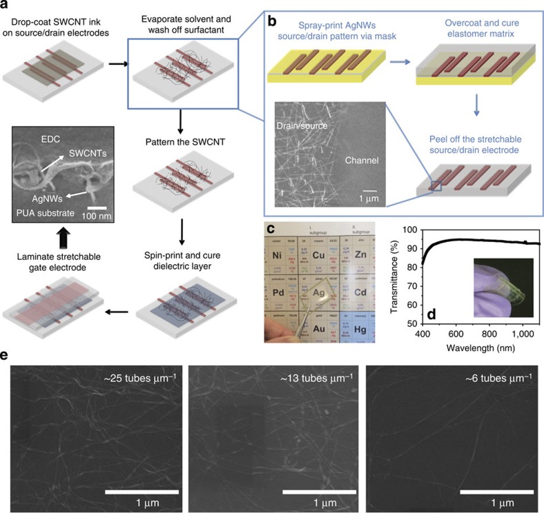
Figure 1. Fabrication process and the SEM and transmittance characterizations of the stretchable TFT.
(a) Schematic illustration of the fabrication steps for a stretchable TFT. The optical microscopic image shows the AgNW-PUA composite source/drain electrodes covered with a SWCNT layer (100 μm channel length). (b) Fabrication process of AgNW-PUA composite source/drain electrodes. Inset: cross-sectional SEM image showing the SWCNTs embedded into and wrapped by the dielectric layer. (c) Optical image of a TFT array marked with a brown dash frame around the element ‘Ag'. (d) Optical transmittance of a TFT array. Inset photograph shows a folded TFT array. (e) SEM images of SWCNT network printed on AgNW-PUA composite source/drain electrodes, showing that the density can be controlled by the amount of SWCNT ink cast on the substrate.

