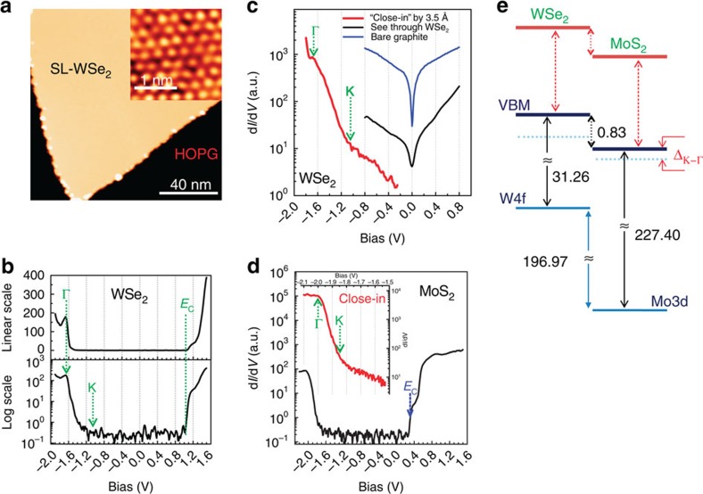
Figure 3. STM images and the tunnelling spectra of WSe2 and MoS2 grown on HOPG.
(a) STM image of single layer WSe2 grown on HOPG. The inset shows the atomic resolution image taken on the SL-WSe2. For the inset, U=−1.4 V, I=10 pA. (b) The dI/dV-V spectrum taken on the SL-WSe2 flake. The tunnelling conductance dI/dV (with arbitrary unit) is plotted in both the linear scale (upper panel) and the logarithmic scale (lower panel). The green dashed arrows indicate the positions of the local VBM at Γ and K points, which are equal to −1.65 eV and −1.05 eV, respectively. The CBM is assigned at +1.03 eV. (c) The clear threshold, corresponding to VBM at K, can be seen in the dI/dV spectrum taken with much more close tip-sample distance (∼3.5 Å closer than b). For comparison, the spectra taken with the stabilization bias with the gap (−0.8 V) is shown in black, while the one taken on bare graphite is in blue. The similar dI/dV (in black) and ‘close-in' (red in inset) spectra of SL-MoS2 are displayed in d, while the valence band maxima at Γ and K are marked in the inset. The EC (blue arrow) corresponds to the CBM. (e) The diagram of band alignments among single-layer MoS2 and WSe2. The local VBM at Γ and global VBM at K are shown in cyan and red, respectively.

