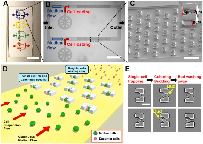
Fig. 1.
Design and working mechanism of the HYAA-Chip for studying aging in yeast. (A) Optical image of the fabricated HYAA-Chip. (Scale bar: 10 mm.) (B) Microscopic image of branched trapping channels linked in parallel. (Scale bar: 1 mm.) (C) SEM of trap arrays in the HYAA-Chip at a 40° tilt angle. (Scale bar: 50 μm.) (Inset) SEM image of a magnified single-trap structure. (D) Schematic view showing the HYAA-Chip working mechanism. (E) Example images of a single yeast cell showing the working mechanism procedure. (Scale bar: 10 μm.)

