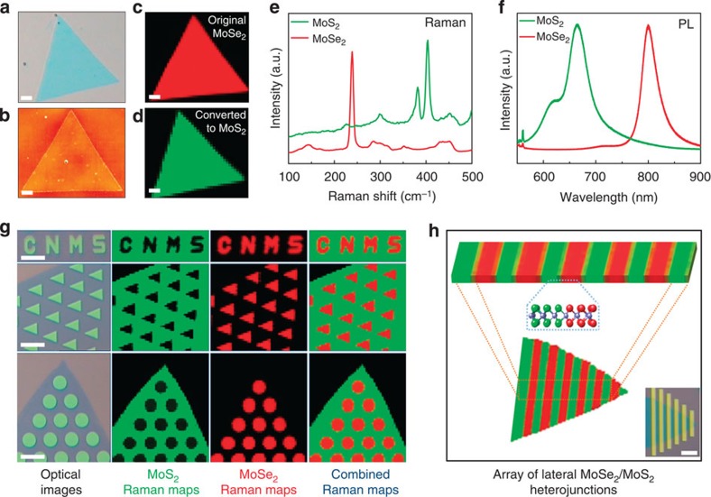
Figure 2. Conversion of MoSe2 to MoS2 and the formation of lateral heterojunction arrays.
(a,b) Optical and atomic force microscopy images of a typical MoSe2 monolayer with a lateral size of ∼40 μm. (c,d) Raman maps of a monolayer nanosheet before and after the complete conversion process (400 pulses at 700 °C), respectively, indicating uniform intensity across the entire crystal. (e,f) Representative Raman and PL spectra of the pristine MoSe2 and converted MoS2 regions. (g,h) Various examples of lateral heterojunction arrays formed within monolayer crystals by patterning and selective conversion processes. The green, red and combined Raman maps are obtained from corresponding optical images, representing the MoS2 (intensity map at 403 cm−1), MoSe2 (intensity map at 238 cm−1) and overlaid MoSe2/MoS2 regions, respectively. Scale bars, 5 μm.

