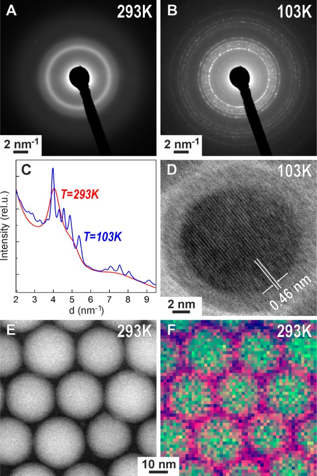
Figure 2.

(A,B) Electron diffraction patterns of ∼32 nm Ga NPs at room temperature and at 103 K. (C) Radial integrals of (A) and (B) indicating the appearance of diffraction peaks upon cooling. (D) High-resolution TEM image of a single Ga NP crystalline at 103 K, coated with a native oxide layer. (E) HAADF-STEM, (F) EDX pseudocolor map of Ga NPs, revealing an O-rich thin shell around a Ga core (Ga, green; O, purple).
