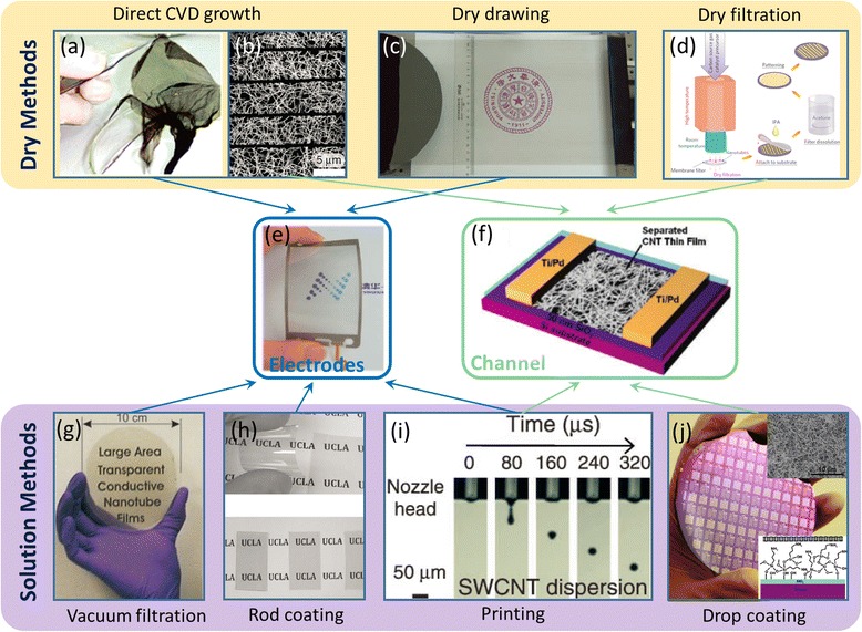
Fig. 1.

Various methods for preparing carbon nanotube networks and representative electronic applications. Dry process (a-d): a Photograph of directly CVD grown freestanding SWCNT thin film. Reproduced from ref. [38]. b SEM image of CVD-grown SWCNT network patterned into strips for channel materials of flexible TFTs. Reproduced from ref. [24]. c Photograph of multi-wall carbon nanotube (MWCNT) thin films obtained using a dry drawing process. Reproduced from ref. [40]. d Schematics of dry filtration process to collect sparse SWCNT network for flexible TFTs. Reproduced from ref. [25]. e, f Applications of carbon nanotube networks as flexible electrodes (e) (reproduced from ref. [37]) or channel materials for flexible TFTs (f) (reproduced from ref. [44]). Solution process (g-j): g Photograph of SWCNT thin film produced by vacuum filtration. Reproduced from ref. [42]. h Photographs of rod-coated SWCNT films with different transmittance. Reproduced from ref. [33]. i Time-dependent snapshot of SWCNT ink droplet during ink-jet printing process. Reproduced from ref. [45]. j Photograph of wafer-scale SWCNT TFTs fabricated using drop-coated SWCNT network. Insets: SEM image of the SWCNT network and schematic illustration of the surface chemistry used. Reproduced from ref. [44]
