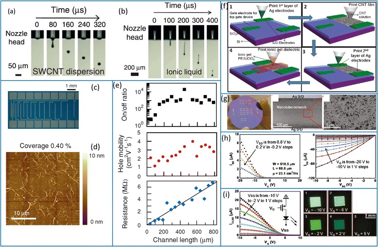
Fig. 12.

Ink-jet-printed SWCNT TFTs. a, b Snapshots of DMF-based SWCNT ink droplet for channel semiconductor (a) and ionic liquid droplet for gate dielectric (b) during the ink-jet printing process. c Optical micrograph of ink-jet-printed TFT array with gold contact electrodes. d AFM image of the printed SWCNT network in the channel of the TFT. e Off/off ratio (top), hole mobility (middle), and channel resistance (bottom) as functions of channel length. Reproduced from ref. [45]. f Schematics of fabricating polymer electrolyte gated SWCNT TFTs by an ink-jet-like process. g Photograph and optical micrograph of fully printed SWCNT TFTs. The SEM image on the right shows the SWCNT network with a high density. h Representative transfer (left) and output (right) characteristics of the fully printed SWCNT TFTs. i Application of printed CNT-TFT in an OLED control circuit. Reproduced from ref. [47]
