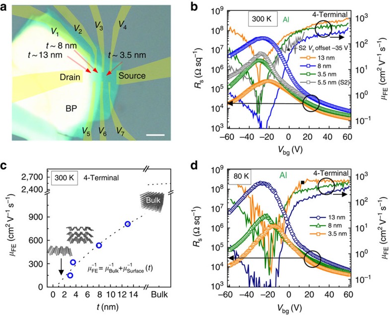
Figure 3. BP thickness dependences of Al-contacted devices.
(a) Optical image of the BP flake (before processing) used for testing layer dependences of transport properties with Al contacts. Yellow shaded region shows locations of electrodes (Supplementary Fig. 3). Scale bar, 3 μm. (b) Rs (open points) and μFE (solid lines) from 4-terminal measurements at 300 K. (c) μFE at 300 K and Vbg=50 V fit to Matthiessen's rule. From fitting, μBulk=2.6 × 103 cm2 V−1 s−1 and estimated monolayer surface scattering is limited to 94 cm2 V−1 s−1. (d) Rs (open points) and μFE (solid lines) from 4-terminal measurements at 80 K. The n-type to ambipolar conversion is observed as the flake thickness increases. Mobility increases with increasing thickness, with n- and p-type μFE∼9.5 × 102 cm2 V−1 s−1 at 80 K for 13 nm thick region (V1,2 in a).

