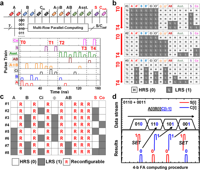
Figure 4. Parallel computing and logic learning.
(a) Array configuration of full adder (FA) circuits and simulated pulse-train waveforms applied at bit lines for adding operation. Different input combinations (input A, B, and carry-in Ci) are stored at multiple rows in the array, operated under the same pulse-train sequence to perform parallel computing. The output results (sum S and carry Co) under various input combinations are stored in situ once computation is finished. (b) Simulated evolution of the cell states during parallel computing procedure for three typical input combinations (#1: 1 + 1 + 1; #2: 0 + 1 + 1; #3: 0 + 0 + 0). T0 to T4 correspond to the five milestone time nodes marked in the waveform of Fig. 2A, among which T0 and T4 are initial and final stages respectively and T1 to T3are all intermediate stages. (c) Complete “knowledge map” learned by FAs after parallel computing. Multiple functions are included in the logic learning, such as AND, XOR and ADD operations. Cells marked by ‘R’ are reconfigurable for other user-defined computing and learning tasks, while the logic functions that are already learned by other cells remain unchanged. (d) Simulated computing results of a 4-bit adder capitalizing on logic learning. For each bit of input, binary A[i]B[i]C[i-1] is decoded (Supplementary Fig. 7) to find the results stored in the “knowledge map” shown in Fig. 4c. The sum S[i] and carry C[i] are read out directly for the following bits.

