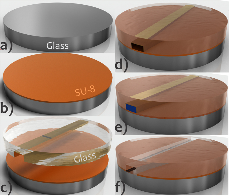
Figure 1. Microfabrication steps for SAB.
Glass slide (a), deposition of SU-8 over this wafer and then pre-bake (b), preliminary bonding against the glass substrate with the walls of the microchannel coated with a thin film of Al (golden in the drawings) (c), cure of the resist just around the microchannel after UV exposure and PEB (resist under the channel is not cured because it is protected from UV by thin film of Al that is deposited only inside the microchannel; see Fig. 4) (d), removal of the uncured SU-8 and, next, of the Al film by pumping specific solvents (blue in the drawing) (e), and final chip showing residual SU-8 in the bottom of the sidewalls (Fig. 6) (f). Features not drawn to scale. In addition, the sidewalls in wet-etched glass are commonly not vertical but rounded.

