Figure 1.
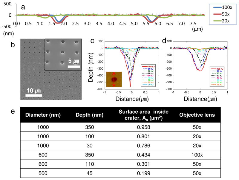
Nanoscale craters were fabricated by direct-write laser ablation lithography. a, AFM contour scans presenting cross sectional images for three different nanocrater dimensions fabricated by 100×, 50×, and 20× objective lenses. There was no evidence of melting or capillarity assisted material movement around the periphery of the crater, since the thermal process exposure was minimized over the short pulse regime. Depending on magnitude of the objective lens, different aspect ratio nanocraters were achieved. b, SEM image of the patterned craters. The inset shows an enlarged patterned surface. c, Cross sectional profiles at the center-line of the ablated nanocraters depending on pulse energies using the 100× objective. Inset image is an AFM top view of a crater showing sectioning line. d, Cross sectional profile of the nanocraters by the 50× objective. e, Dimensions of nanocraters for creating the gradient patterns. Six different dimensions of nanocrater gradient patterns were fabricated by using 100×, 50× and 20× objective lenses. The surface area inside crater was calculated based on diameter and depth with assuming the craters are conical shape.

