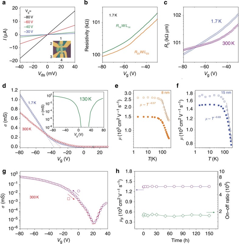
Figure 2. Mobility and stability of the BN–BP–BN heterostructure devices.
(a) The I–Vds curves obtained at different gate voltages at 1.7 K. The inset is the optical image of Sample A with the following geometrical parameters: L14=16 μm, L23=10 μm and W=3 μm. (b) The resistivity determined from four-terminal (green line) and two-terminal configurations (orange line) at 1.7 K. (c) Variation of the contact resistivity. (d) The conductivity of Sample A measured at with a room temperature and 1.7 K. The inset shows the ambipolarity of the BP conductance. (e,f) Temperature dependence of the field-effect μF (open dots) and Hall mobilityμh (solid dots) at Vg=−70 V) of Sample A and Sample B (15 nm thick). The dashed lines serve as guidelines for the μ∼T−γ relation. (g) The room temperature conductivity showing no hysteresis in Sample A. (h) The mobility and on–off ratio of Sample A as a functions of ambient exposure time. No quality degradation is observed even after exposure for an entire week.

