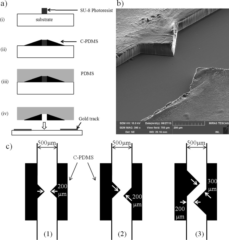
FIG. 1.
(a) Fabrication process: (i) photolithography, (ii) C-PDMS deposition, (iii) PDMS pouring, and (iv) demolding and plasma bounding on glass substrate. (b) SEM picture of C-PDMS electrodes before sealing; visible asperities on the surface of C-PDMS electrodes can be explained by the paste-like behavior of C-PDMS during molding. (c) Illustration of the three configurations of electrodes realized: (1) face-to-face, (2) slightly shifted, and (3) shifted.

