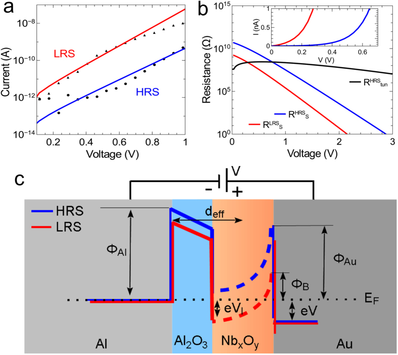
Figure 4. Schematic of the electronic band structure variations.
(a) I–V characteristics of the LRS and HRS branch of the double barrier device in the reverse voltage regime of the Schottky contact (device area is normalized to 1 μm2). Solid lines are data fits according to Equation 1 to extract the Schottky barrier height ϕB. (b) Comparison between the Schottky contact resistance at the LRS and HRS branch and the tunnelling resistance. Inset: Shift of the diode forward current onset. (c) Schematic electronic band diagram of the double barrier structure for the LRS (red line) and HRS (blue line). During the transition from the HRS to LRS, moving oxygen ions cause an decrease of the interfacial potential VI by a down shift of the interfacial band in NbxOy (dashed line). Further, the effective barrier tunnel width deff and the apparent barrier heights ϕAl, and ϕAu of ,respectively, the Al electrode, and Au contact are decreased.

