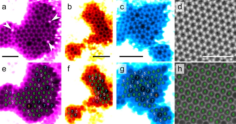
Figure 2.
Atomic-resolution images of amorphized graphene areas. (a–d) Example STEM-MAADF images from the amorphized areas (a–c) and a pristine area (d). A deconvolution with the beam profile, modeled as a sum of two Gaussians, has been applied as described in ref (36), followed by a Gaussian blur for panels (a–c) with a radius of 2–3 pixels. (e–h) Same images after the application of a minimum filter with a radius of 10 pixels to enhance the visibility of the nonhexagonal rings with the size of each ring marked on top of the rings. The marked atoms in panel (a) were identified as Si based on the contrast in the MAADF images. The bright areas around the atomically thin structures are covered by hydrocarbon contamination. All scale bars are 1 nm. Each pair of images is colored uniquely to ease the comparison.

