Figure 3.

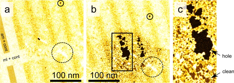
Chemical etching of the amorphous pattern. (a) STEM-MAADF close-up image of a patterned area of the sample before and (b) after an exposure of about 1 h to a parallel electron beam while air was leaked to the objective area of the microscope column (pressure increase from ca. 5.3 × 10⁻⁹ to 1.1 × 10⁻⁶ mbar). The approximate area exposed to the beam corresponds to the darkened circular shape seen in panel (b). Partial overlay on the left-hand-side of panel (a) highlights the structure of the pattern (“ml+cont” corresponds to nonirradiated graphene and contamination, whereas “am+cont” refers to amorphized areas). Circles with solid and dashed lines mark the same hole and metal contamination, respectively, in both images to ease the comparison. A higher magnification of the area marked with a rectangle in panel (b) is shown in panel (c) to ease distinguishing holes and clean graphene from each other.
