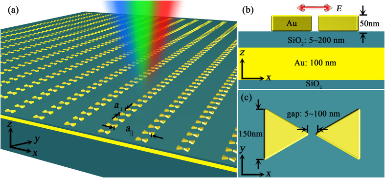
Figure 1. Schematic of the plasmonic BNAs and single bowtie antenna with MIM configuration.

(a) Schematic of the Au BNAs with MIM configuration. (b) Front view and (c) top view of a single bowtie nanoantenna. The thickness and length of the Au equilateral triangles are 50 nm and 150 nm, respectively. The gap between the tips of the two triangles ranges from 5 to 100 nm. A SiO2 spacer layer with the thickness ranging from 5 to 200 nm lies below the BNAs. An Au thin film is sandwiched between the spacer layer and the SiO2 substrate. The thickness of the Au thin film is set as 100 nm, which totally blocks the light transmission through the structure.
