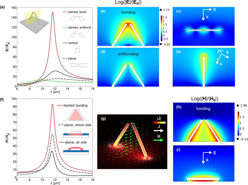
Figure 3.
Comparison of electric (a–e) and magnetic (f–i) properties of the slanted nanorod dimer with reference structures. The slanted dimer geometry and illumination considered are depicted in (a), left inset. It has the same geometrical parameters as in Figure 1 except for β = 180°. (a) Comparison of electric FEs spectra for the structures (b–e). Fields are taken in representative positions, as schematized in the legend. The red curve denotes the field at the gap center of the slanted dimer for TE-polarized illumination and scattering plane as depicted in the inset. The green curve is the FE for the same structure with TM-polarized illumination and calculated 50 nm above the antenna terminations. The solid black line is the FE in case of vertical antenna on silver substrate, calculated 50 nm above the antenna edge; the black dashed line is the FE at the center of a planar dimer antenna on silicon substrate with gap size of 100 nm. (f) Comparison of the maximum magnetic FE for the slanted dimer bonding resonance (red line) with the maximum FEs in case of a planar silver antenna on 70 nm thick silicon layer on a silver substrate. Field maxima are calculated over the respective spatial regions shaded with red in the schematics. (g) Surface current distributions (white arrows and color map) and magnetic field in the middle plane (green arrows) for the slanted dimer at bonding resonance. (h,i) Magnetic FE maps at resonant wavelengths. The lengths of the reference structures considered (c,e,i) have been tuned in order to resonate at the same wavelength of the slanted antenna bonding resonance. They are 1800 nm for (c), 2450 nm for (e), and 1700 nm for (i).

