
Figure 7. Modelling the mud-cracking of metallized, oxygen plasma-treated PDMS.
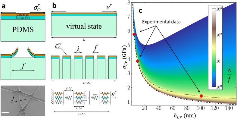
(a) schematic diagram showing film having residual tensile stress  (top) and cracked film having crack width f (middle), and SEM image of a cracked PDMS/SiOx/Cr film – scale bar = 5 μm (bottom). (b) schematic diagram showing pre-cracked, virtual state (top) and cracked state (middle), and mechanical model of the multi-layer (bottom). (c) modelling of crack spacing-to-crack width ratio (λ/f) as a function of chromium thickness
  and chromium stress level
  . Experimental values are shown as red circles for 5 nm, 10 nm and 100 nm thick chromium films. The dashed lines are explained in the text.