
Fig. 2.
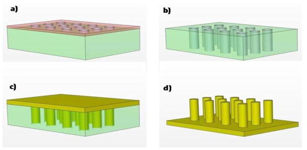
Micropost array fabrication process, a) after photolithography and patterning circles which corresponds to post diameter, b) after deep Si etching to create Si mold with high aspect ratio, c) after pouring and curing PDMS, d) after peeling off cured PDMS from the mold.