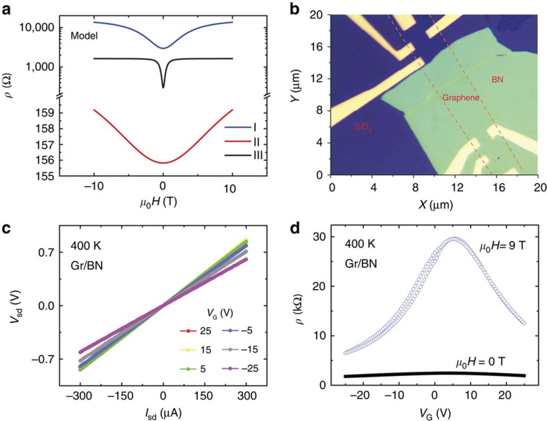
Figure 1. Electric and magnetic field effect of channel resistivity in few-layer graphene.
(a) Resistivity versus external magnetic field (H) based on the theoretical prediction for a certain combination of carrier densities and mobilities in two effective channels, suggesting the possibility of very high magnetic field sensitivity at moderate magnetic fields. Case I: n1=1011 cm−2, n2=1.1 × 1011 cm−2, μ1=20,000 cm2 V−1 s−1, μ2=1,000 cm2 V−1 s−1; case II: n1=8 × 1012 cm−2, n2=1.1 × 1011 cm−2, μ1=5,000 cm2 V−1 s−1, μ2=1,000 cm2 V−1 s−1; and case III: n1=1011 cm−2, n2=1.1 × 1011 cm−2, μ1=200,000 cm2 V−1 s−1, μ2=10,000 cm2 V−1 s−1. (b) Optical micrograph of the fabricated four-layer graphene (Gr) on top of BN and SiO2. The location of Gr is indicated by red dashed lines. (c) The voltage (Vsd) as a function of source-drain current (Isd) at various gate voltages (VG) suggesting an ohmic contact for Cr/Au electrodes on Gr. (d) The channel resistivity (ρ) as a function of VG at 400 K. A magnetic field of 9 T is also applied normal to the Gr plane.

