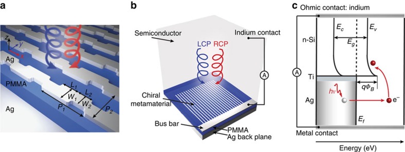
Figure 1. Schematic of the chiral metamaterial and the CPL detector.
(a) Schematic of the chiral metamaterial consisting of the chiral plasmonic meta-molecule array, dielectric spacer and metal backplane. The dimensions of the meta-molecules are L1=125 nm, L2=105 nm, W1=115 nm, W2=85 nm, P1=335 nm and P2=235 nm. The thickness of the meta-molecules, dielectric spacer and the metal backplane are 40, 160 and 100 nm, respectively. (b) Schematic of the CPL detector consisting of a chiral metamaterial integrated with a semiconductor that serves as a hot electron acceptor. The Ohmic contact on Si is formed by soldering indium. The circuit is formed by wire bonding to the silver bus bar and indium. (c) Energy band diagram of the CPL detector. A Schottky barrier is formed between Si and the Ti interfacial layer. The hot electrons that are photo-generated in the Ag metamaterial are then injected over this barrier into the Si.

