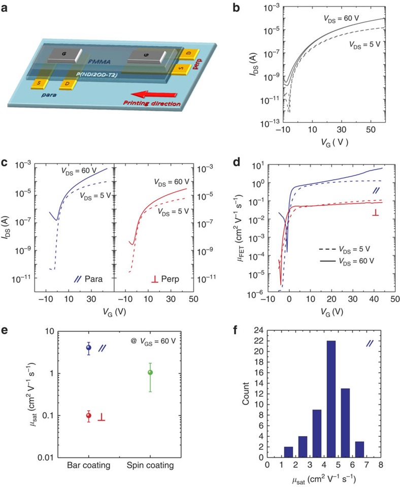
Figure 3. Electrical properties of FETs.
(a) Sketch of the top gate bottom contact FETs structure employed; the probing directions are clearly represented with respect to the printing direction and indicated as para (printing parallel to the source to drain electric field) and perp (printing perpendicular to the source to drain electric field). (b) Typical transfer characteristic in linear (dashed) and saturation (continuous) regime of a submonolayer based FETs with W=2 mm and L=20 μm; currents ON/OFF ratio is ∼106 in the linear regime. (c) Typical transfer characteristic plots in linear (dashed) and saturation (solid) regimes of 10 nm thick film based FETs with W=2 mm and L=20 μm with the fibrils axis oriented parallel (blue) and perpendicular (red) to the probing direction; in the linear regime, currents ON/OFF ratio is ∼107 for the parallel case and ∼106 for the perpendicular case. (d) Typical effective linear and saturation mobility as a function of the gate voltage in the perpendicular and parallel direction: the anisotropy is marked both with a high and a low lateral applied voltage. (e) Average saturation mobilities (circles) with their standard deviation (bars) for 56 FETs coated on an 8 × 8 cm2 area in both parallel and perpendicular directions, compared to a distribution obtained from 8 spin-coated FETs. (f) Distribution of the saturation mobility in the parallel case for 56 FETs coated on an 8 × 8 cm2 area.

