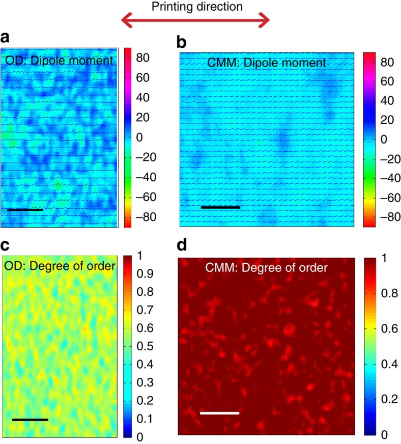
Figure 5. Polarized optical density and charge modulation microscopy maps.
13 × 24 μm2 polarized optical density (OD) map (a) and 18 × 18 μm2 CMM map (b) with the indication of the polymers backbone orientation (black dashed lines) and the relative degree of orientational order maps (c,d) of a bar-coated film. On the top of the picture the direction of printing with respect to the maps is reported. Scale bars, 4 μm. The mean DR values are calculated relative to these scanned areas.

