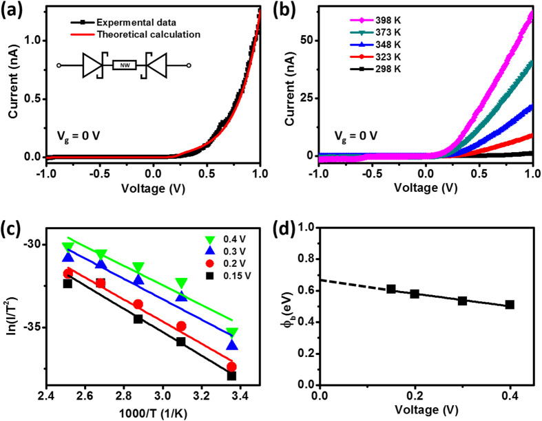
Figure 3.
(a) I–V curve (black) and fitted data (red) of a ZnO NW Schottky device. The inset shows the circuitry of the back-to-back Schottky device. (b) I–V curves of the Schottky device measured at temperatures ranging from 298 to 398 K. (c) Plots of ln(I/T2) versus 1000/T at various applied voltages; the data had been extracted from (b). (d) Values of φb plotted with respect to the applied voltage.

