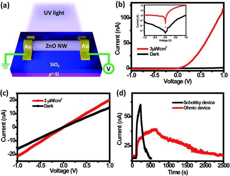
Figure 4.
(a) Schematic representation of a ZnO device illuminated with UV light. (The figure was drawn by Shuen-Jium You) (b) I–V characteristics of a Schottky device in the dark (black) and under 365-nm UV light (red); inset: the same data plotted on a logarithmic scale. (c) I–V characteristics of an ohmic device in the dark (black) and under 365-nm UV light (red). (d) Photoresponses of the ZnO NW Schottky (black) and ohmic (red) devices under illumination with UV light at a power density of 1 μW/cm2.

