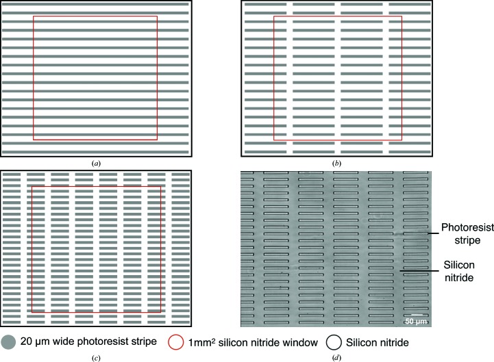
Figure 3.
Photoresist stripe-based chip designs. (a, b, c) Schematic representation of the design masks for patterning a 1 mm2 silicon nitride window with 20 µm wide photoresist structures of varying lengths. (d) Optical micrograph of an area within a single 1 mm2 silicon nitride window patterned with 20 µm wide by 137.5 µm long photoresist structures.

