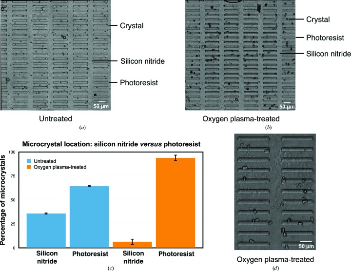
Figure 4.
Optical imaging of HEWL microcrystals sealed in untreated and oxygen plasma-treated three-layer chips. (a) Light micrograph of a 1 mm2 silicon nitride window patterned with 20 µm wide, untreated photoresist stripes loaded with HEWL microcrystals. (b) Light micrograph of a 1 mm2 silicon nitride window patterned with 20 µm wide, oxygen plasma-treated photoresist stripes loaded with HEWL microcrystals. (c) Quantification of HEWL microcrystal number optical imaging within the bounds of a 1 mm2 silicon nitride window. (d) Close-up view of crystals within an oxygen plasma-treated chip.

