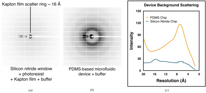
Figure 6.
Comparison of background scattering between silicon nitride-based and PDMS-based devices. (a) Diffraction image from a three-layer (silicon nitride window, 15 µm thick photoresist and Kapton film) device containing crystallization buffer. The dark scattering ring at 16 Å resolution derives from the Kapton film. (b) Diffraction image from a ∼100 µm thick two-layer microfluidic PDMS crystal capture device loaded with crystallization buffer. (c) Plot of scattering intensity versus resolution for the images shown in (a) and (b). The cone-shaped dark area to the left of the beamstop corresponds to the part of the diffraction image where X-rays were not blocked by the X-ray scatter guard. Data for (c) were smoothed to remove sharp features caused by these unblocked X-rays.

