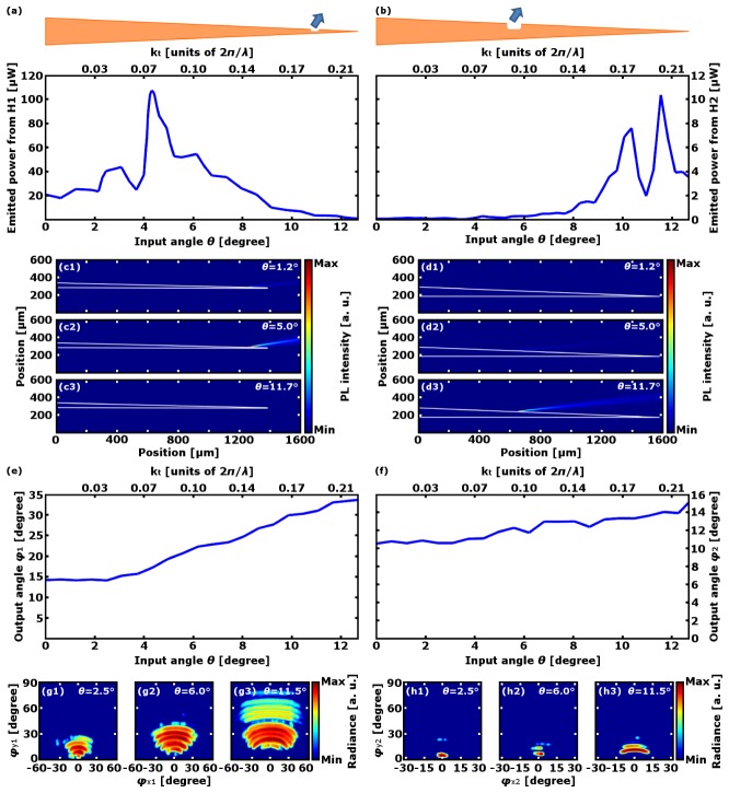
Fig. 4.
(a), (b): Power emitted from devices W1 (panel a) and W2 (panel b) as a function of θ for input power of 15 mW. (c), (d): Fluorescence images of the emission of devices W1 (panel c) and W2 (panels d) for three different values of θ, the taper being submerged in a fluorescein droplet. White lines show the taper profile. (e), (f): Outcoupling angle of the light emitted from device W1 (panel e) and W2 (panel f) as a function of θ. (g), (h): Normalized radiance maps of the light emitted from devices W1 (panels g) and W2 (panels h) obtained through the ray tracing model for three different values of θ. Definitions of φx and φy are reported in Fig. 2(c). For each map the colorbar represents a 6 decades logarithmic scale.

