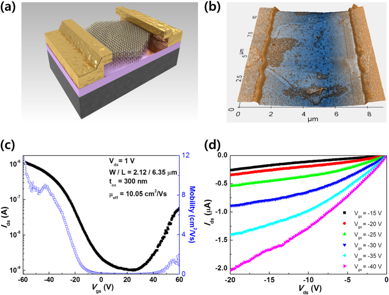
Figure 3. Thin-film transistor based on the CVD-synthesized hexagonal MoSe2 multilayer.
(a) 3D schematic structure for TFT based on hexagonal multilayer MoSe2 film. (b) 3D topography AFM image of the hexagonal MoSe2 TFT with a channel length of 6.35 μm. (c) Transfer (Ids − Vgs) curve and field-effect mobility (μeff) of the hexagonal MoSe2 TFT (−60 ≤ Vgs ≤ 60 V at Vds = 1 V). (d) Output characteristics of the respective device (−20 ≤ Vds ≤ 0 V, −15 ≤ Vgs ≤ −40 V in steps of −5 V).

