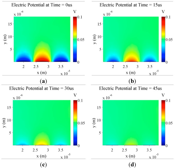
Figure 3.
Simulation of the formation of electrical screening layers over time. Plots show the electric potential of IDEs (5 µm digit width and 2.5 µm spacing) with 0.1 V DC applied with a background KCl concentration of 150 µM. Plots are taken at five different time points: (a) t = 0 s; (b) t = 15 µs; (c) t = 30 µs; (d) t = 45 µs.

