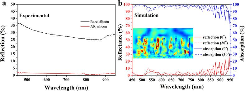
Figure 6.

(a) Reflectance spectra of bare silicon wafer and AR wafer from 450 to 950 nm. The reflectance of AR wafer is under 3%. (b) Simulated optical reflection and absorption spectra of AR wafer with the incident angle of 0° and 30°, respectively, and the inset shows the typical electric field distribution at the wavelength of 730 nm.
