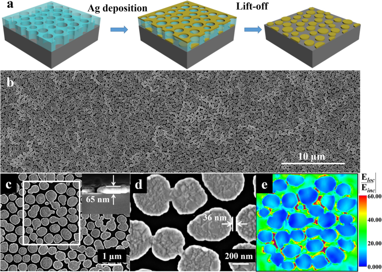
Figure 7.
(a) Schematic of fabricating SERS-active substrate by the lithography process based on phase separation method. (b–d) present the top view of SEM images of Ag nanodot arrays with different magnification, respectively. The inset of (c) is the cross-sectional view of SEM image of a typical Ag nanodot with thickness of 65 nm. The distance between every two Ag nanodots is about 36 nm. (e) The calculated distribution of enhancement ratio of local electric field  under the laser excitation with wavelength of 532 nm. The purple area stands for the enhancement ratios of local electric field which are greater than 60.

