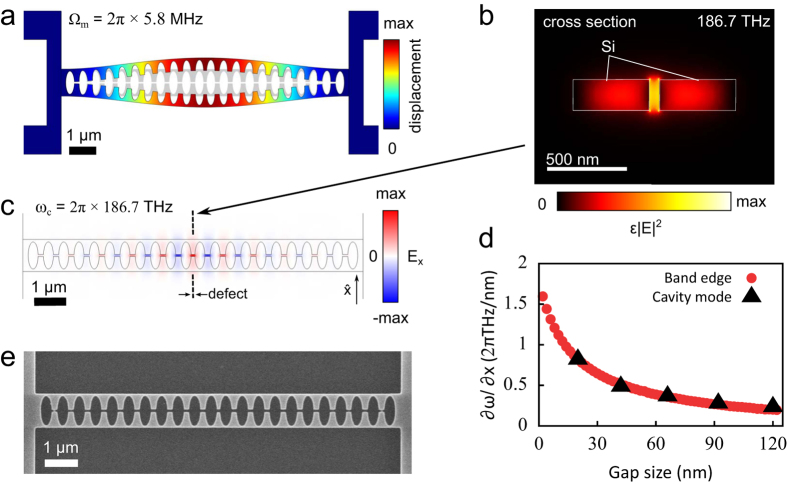
Figure 1. Resonances and geometry of the sliced nanobeam.
(a) Simulated displacement profile of the fundamental (in-plane) mechanical resonance of the structure. (b) Cross section in the center of the sliced nanobeam (indicated by the dashed line in c), showing the simulated energy density distribution of the fundamental optical cavity mode of the structure. (c) Simulated transverse electric field profile of the fundamental optical cavity mode of the structure. (d) Simulated frequency shift as a result of an outward displacement of 1 nm. The cavity mode shift was determined by simulating the full nanobeam and introducing a uniform displacement along the beam. (e) Electron micrograph of a fabricated device. The thickness of the structure is 200 nm, both in the simulations and in the fabricated device.

