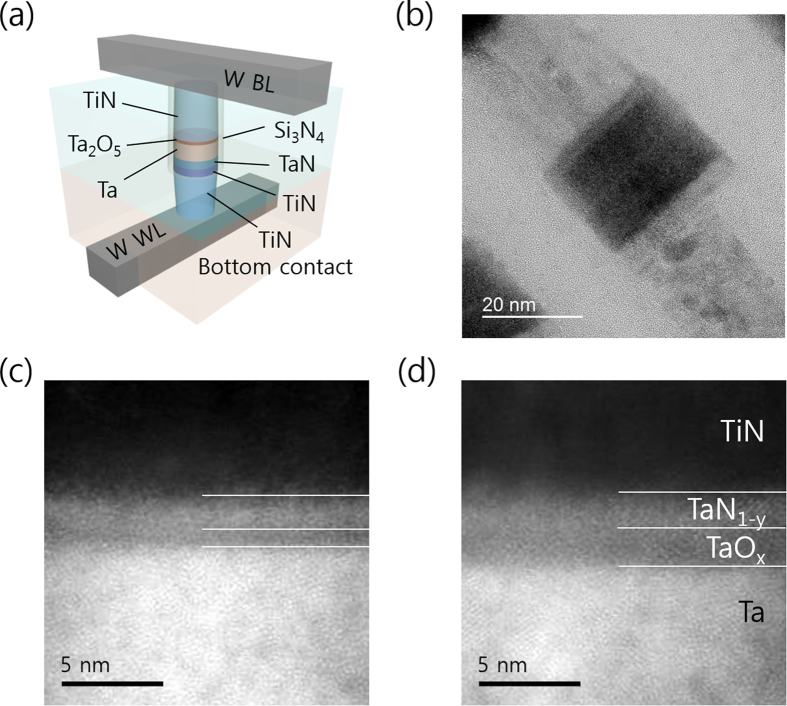
Figure 1.
(a) Schematic diagram and (b) TEM image of the TiN/Ta2O5/Ta/TaN device. Ta2O5 (0.5 nm) device, and (d) Ta2O5 (1.5 nm) device. Insets show the linear I-V plot. Scanning transmission electron microscopy (STEM) high angle annular dark field (HAADF) images of (c) 0.5 nm-thick device and (d) 2.0nm-thick device.

