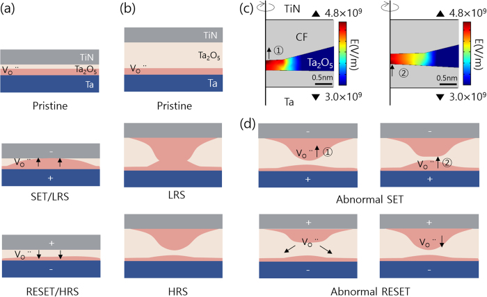
Figure 4.
Schematic diagram of the memory cell at the pristine (upper panel), LRS (middle panel) and HRS (lower panel) of the device with tTaO of (a) 0.5 nm (b) 1.5 nm. (c) Electric field distribution, calculated by COMSOL package. (d) Schematic diagrams depicting abnormal SET (upper two panels), and abnormal RESET (lower two panels) behaviors.

