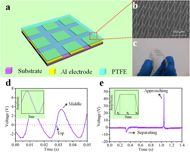
Figure 1. Structure illustration and typical electrical response of the active sensor system.
(a) The schematic diagram of the active sensor system. (b) The SEM image of the PTFE film with patterned microstructure. (c) Photograph of a bent flexible device. Photograph taken by Qijie Liang. (d,e) Output voltage with different loading process.

