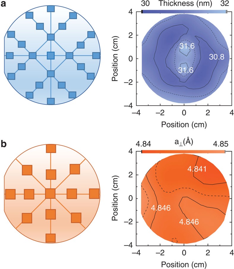
Figure 3. Wafer-scale metrology of VO2 grown on a 3-inch r plane sapphire substrate.
The squares in the schematic on the left represent the probing locations on the wafer. (a) Film thickness uniformity extracted from spectroscopic ellipsometry measurements. (b) Map of the out-of-plane lattice parameter determined from X-ray diffraction scans.

