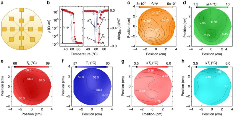
Figure 4. Wafer-scale mapping of MIT properties of 3-inch VO2.
(a) Schematic with squares showing the probing locations on the wafer. (b) Definition of the MIT properties: resistivity ratio (Δρ/ρ), transition point (Th and Tc), transition sharpness (ΔTh and ΔTc) and transition width (ΔH). The subscripts h and c indicate the cooling and heating cycle, respectively. Closed red and open blue circles represent heating and cooling cycles, respectively. (c) Map of VO2 resistivity ratio Δρ/ρ=(ρ30 °C−ρ80 °C)/ρ80 °C obtained from four-point–probe measurements of resistivity ρ30 °C at 30 °C (VO2 insulating state) and ρ80 °C at 80 °C (VO2 metallic state). Wafer-scale mapping of MIT properties defined in b across the 3-inch VO2 film: (d) ΔH, (e) Th, (f) Tc, (g) ΔTh, (h) ΔTc.

