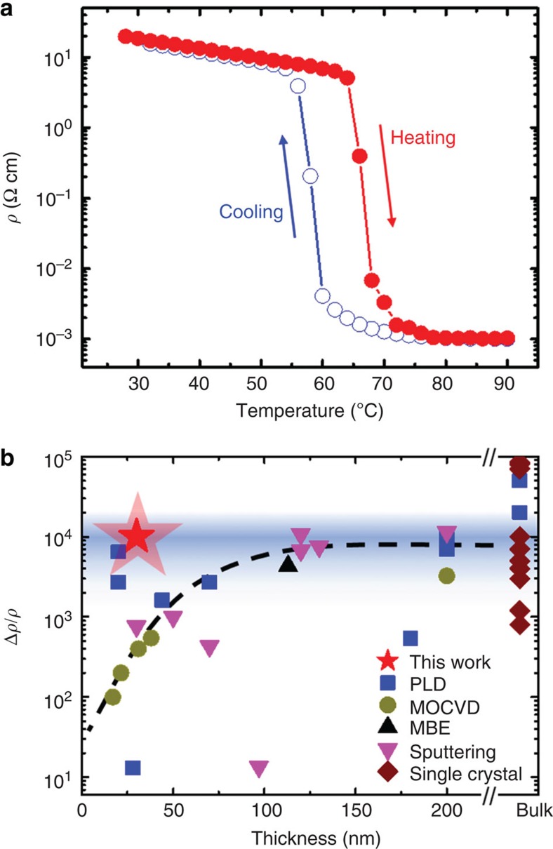
Figure 6. Benchmark of VO2 thin films.
(a) Temperature-dependent resistivity of VO2 films grown under optimized condition on a 3-inch r plane Al2O3. Measurement was taken at the wafer center. (b) Benchmark of resistivity ratios Δρ/ρ=(ρ50 °C−ρ80 °C)/ρ80 °C for VO2 across the metal-to-insulator transition. Note that the low temperature resistivity was taken at 50 °C. For a direct comparison, all films were grown on Al2O3 substrates above the critical films thickness. The blue-shaded area indicates the highest values reported for VO2 films on sapphire and typical values obtained in bulk single crystals. A dotted line was added as guide to the eye. Note the two PLD samples with resistivity ratios higher than Δρ/ρ=103 at film thicknesses <25 nm, from ref. 21. A thickness much >200 nm was estimated for the VO2 films grown by PLD in ref. 57 and the data were added as ‘bulk' value. Data for bulk VO2 were taken from refs 47, 48, 49, 50, 51, 52, 53. Properties of VO2 films on Al2O3 substrate grown by PLD were taken from refs 21, 42, 52, 53, 54, 55, 56, 57, MOCVD from refs 58, 59, MBE from ref. 27 and sputtering from refs 8, 23, 25, 60, 61, 62, 63.

