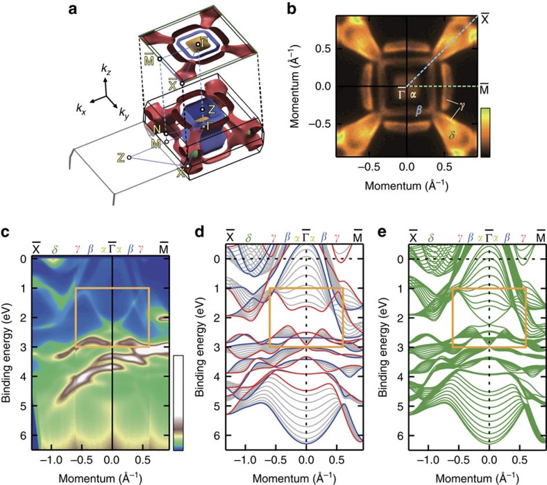
Figure 2. Electronic structure of β-PdBi2.
(a) Calculated Fermi surfaces shown with the first Brillouin zone. kx, ky and kz axes for the crystal momentum space are depicted. Γ, Z, N, X and M are the high-symmetry points. The square plane represents the two-dimensional (2D) projected surface Brillouin zone with 2D high-symmetry points,  ,
,  and
and  . (b) Four-fold symmetrized Fermi surface recorded by angular-resolved photoemission spectroscopy (ARPES). The image is obtained by integrating intensities in the energy window of ±8 meV at the Fermi level. The colour scale indicates the intensity. Two electron-like and two hole-like Fermi surfaces are denoted by α, β and γ, δ, respectively. (c) ARPES image recorded along
  –
– and
and  –
– cuts, shown as the light-blue and -green broken lines in b, respectively. The colour scale indicates the intensity. (d) Calculated bulk band dispersions projected onto 2D surface Brillouin zone. Blue (red) curves correspond to kz=0 (2π/c). (e) Surface band dispersions obtained by slab calculation of 11 PdBi2 layers. Orange rectangles in c–e indicate the region where the surface Dirac cone appears.

