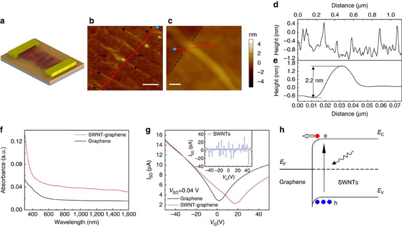
Figure 1. Planar SWNT–graphene hybrid film and photodetector.
(a) Schematic of the phototransistor. (b) AFM image of the hybrid film on the SiO2/Si substrate (Scale bar, 200 nm). Black arrows are used to pinpoint individual SWNT. (c) AFM image of one individual SWNT partially covered by graphene (Scale bar, 20 nm). SWNT was uncovered by mechanically exfoliating the top graphene using a tape stripe. The black dashes show the edge of the graphene (left: SiO2; right: graphene). (d) Height profile along the red line in b. The blue dot in b marks the zero point in d. (e) Comparison of the respective height profiles of the graphene-covered portion and the uncovered portion of SWNT shown in panel c. (f) Ultraviolet–visible-infrared absorbance curves of graphene and SWNT–graphene hybrid film on quartz. (g) Transfer characteristics of the graphene, SWNTs and SWNT–graphene transistors without light. Comparing with the graphene transistor, the Dirac point of the SWNT–graphene transistor shifted from 2 to 17 V, indicating p-type doping in the graphene sheet induced by SWNTs. The electron (hole) mobility decreases from 6,142 cm2 V−1 s−1 (7,146 cm2 V−1 s−1) to 3,771 cm2 V−1 s−1 (4,666 cm2 V−1 s−1). The inset exhibits that the source-drain current of the SWNTs transistor is <10−11 A, indicating disconnected electric pathways for the pristine SWNTs channel. (h) The energy band diagram at the junction formed by graphene and semiconducting SWNTs. Photogenerated electrons in SWNTs are transferred to graphene due to the built-in field at the junction.

