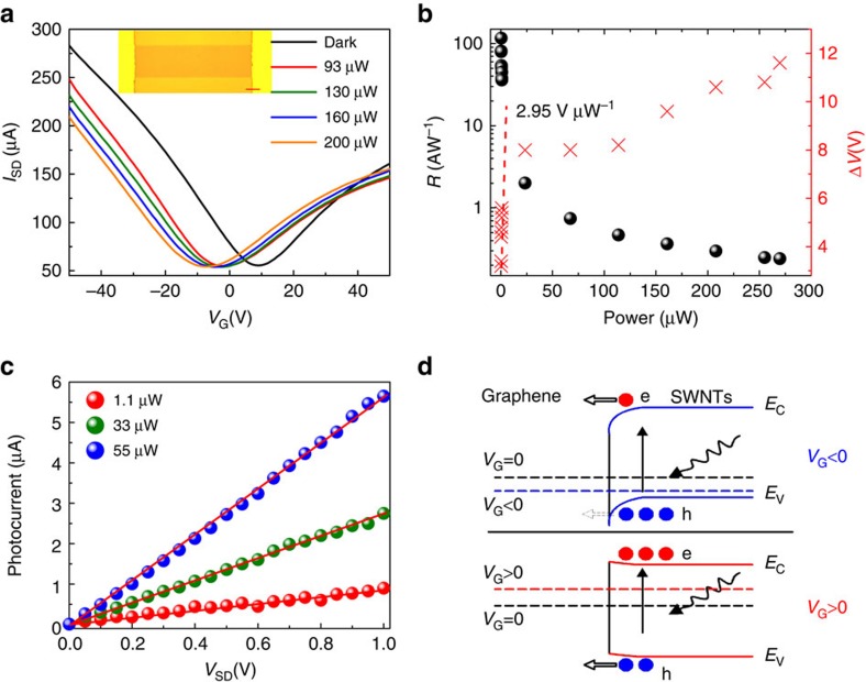
Figure 2. Photoresponse performance under 650 nm illumination.
(a) Source-drain current (ISD) as a function of back-gate voltage (VG) for the SWNT–graphene device with increasing 650 nm illumination intensities. VSD=0.5 V. Increasing of the illumination leads to a photogating effect that shift the Dirac point to lower VG, indicating electron doping of the graphene sheet. The inset is the optical micrograph of the fabricated device (Scale bar, 10 μm). The gold areas indicate the metal electrodes. The orange area and LT orange areas are graphene channel and SiO2/Si substrate, respectively. (b) Responsivity (black dots) and shift of Dirac point (red cross) as a function of the 650 nm illumination. (c) The magnitude of the photocurrent increases linearly with source-drain bias voltage (VSD) for different optical powers (VBG=0). Red lines are linear fits. (d) Energy-band diagram of the SWNT–graphene phototransistors at different back-gate voltage. The dash lines correspond to the Fermi level of graphene at different gate voltages. The blue and red lines schematically illustrate the gate voltage dependence of the SWNT energy levels.

