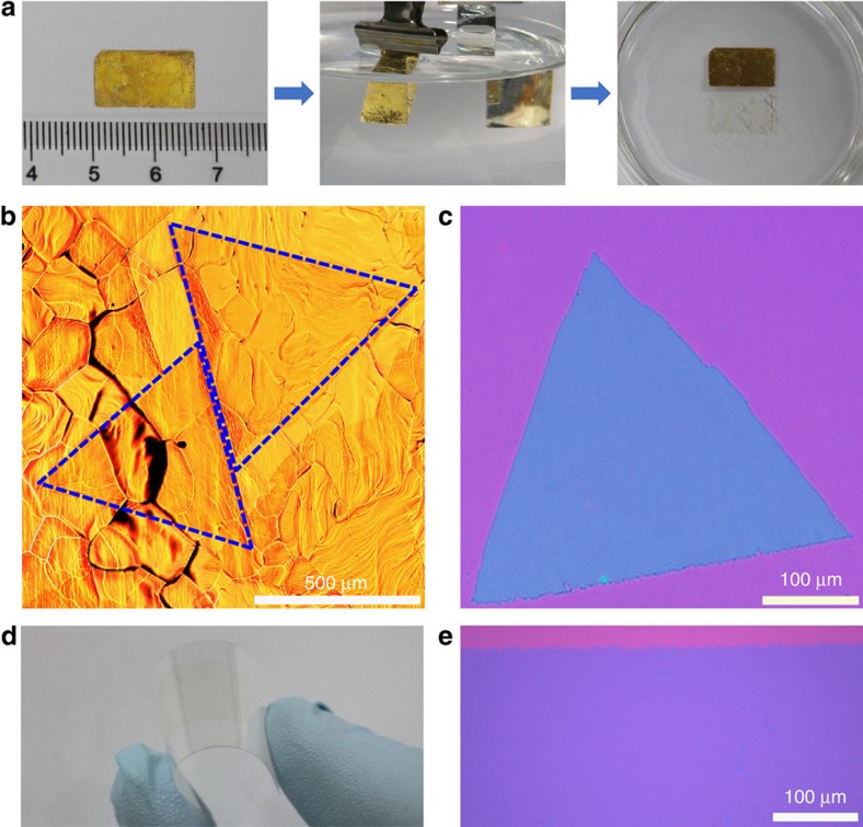
Figure 1. CVD growth of monolayer WS2 single crystals and films on Au foils and electrochemical bubbling transfer.
(a) Electrochemical bubbling transfer of the monolayer WS2 grown on a Au foil by ambient-pressure CVD. Left panel, the Au foil with monolayer WS2 covered by a polymethyl methacrylate (PMMA) layer. Middle panel, the PMMA/monolayer WS2 was gradually separated from the Au foil driven by the H2 bubbles produced at the cathode when applying a constant current. Right panel, the completely separated PMMA/monolayer WS2 and Au foil after bubbling for 30 s, showing the intact Au foil. (b) Optical image of millimetre-sized triangular monolayer single-crystal WS2 domains on the Au foil. (c) Optical image of a 400-μm single-crystal WS2 domain transferred on a SiO2/Si substrate. (d) Photograph of a monolayer WS2 film transferred on a PET substrate, showing good flexibility. (e) Optical image of the edge region of a monolayer WS2 film transferred on a SiO2/Si substrate, showing uniform thickness without any additional layers and visible cracks.

