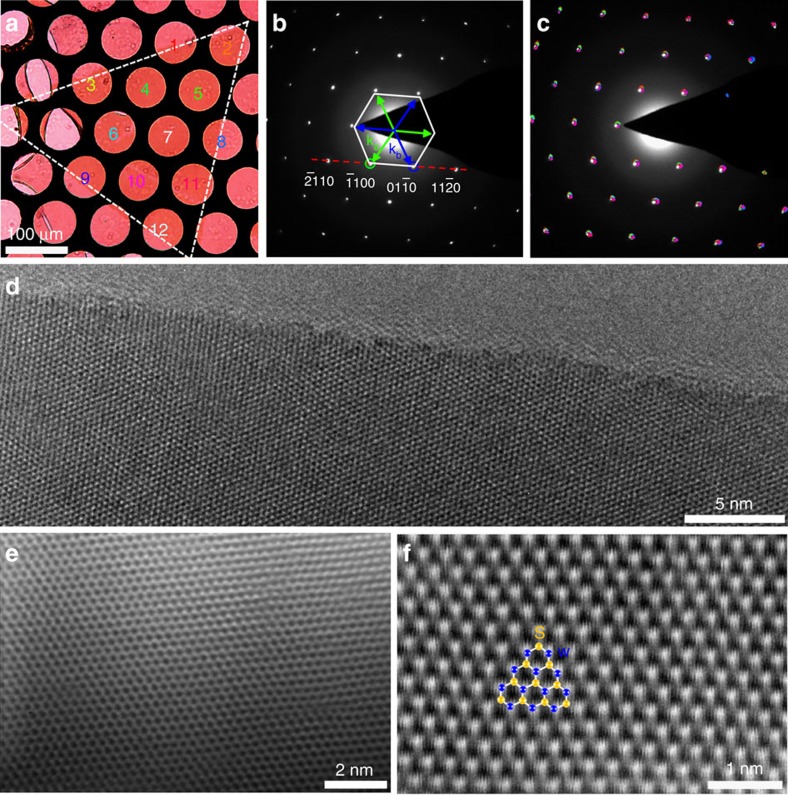
Figure 2. Structural characterization of monolayer single-crystal WS2 domains.
(a) Optical image of a 400-μm monolayer WS2 domain transferred on a TEM grid. (b) Typical SAED pattern of the sample in a showing a hexagonal crystal structure. The asymmetry of the W and S sublattices separates the  diffraction spots into two families:
  and kb=−ka. (c) Superimposed image of 12 coloured SAED patterns taken from the areas labelled with numbers 1–12 in a. The same colours were used to indicate the SAED patterns and the corresponding areas in a, where they were collected. (d–f) HRTEM (d) aberration-corrected HRTEM, (e) aberration-corrected ADF-STEM (f) images of the monolayer WS2 domains, showing no point defects, voids and sulphur vacancies.

